Coating thickness gauge EddyCus® TF map 5050SR non-contactfor aeronauticseddy current
Add to favorites
Compare this product
fo_shop_gate_exact_title
Characteristics
- Applications
- coating
- Technology
- non-contact
- Other characteristics
- for aeronautics, eddy current
- Measuring range
Min.: 2 mm
(0.08 in)Max.: 10 mm
(0.39 in)
Description
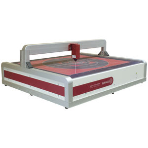
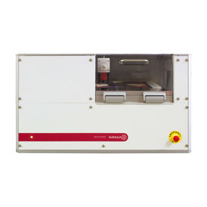
The EddyCus® TF map 5050 Series is a high-resolution non-contact imaging device series for sampling areas up to 500 x 500 mm (20 x 20 inch). The bench-top device automatically measures at various measurements points, typically with a pitch in X and Y of 1 mm (40 mil) generating accurate mappings. The system acquires hundreds of measurements per second on the fly resulting in high resolution images containing up to 250,000 measurement points per sample. The bench-top devices allow depending of its setup the precise imaging of metal thickness, sheet resistance or electrical anisotropy. The resulting property images provide a deep insight to layer homogeneity and defect density and hence offer a profound basis for material and process optimization. Applications involve quality assurance for sputtering, evaporation, ALD, CVD, electroplating or doping and annealing processes.
Highlights
Non-contact imaging
Fast and accurate
High resolution imaging with 1 mm pitch (alternatively 0.25 to 10 mm)
Sampling areas of 500 x 500 mm (20 x 20 inches)
Advanced layer uniformity analysis and defectoscopy
Characterization of hidden and encapsulated conductive layers
Profound software-integrated analysis functions (line profiles, histogram analysis, selective area analysis, statistics)
Hybrid systems (e.g. combined electrical and optical imaging)
Systematic quality control, incoming inspection, inspection of outgoing goods
Types
Devices are offered with different sensor configurations using eddy current sensors of optical components.
Characteristics
Technology: non-contact eddy current sensor
Sampling area: 500 x 500 mm
Catalogs
No catalogs are available for this product.
See all of SURAGUS GMBH‘s catalogsRelated Searches
- Laser scanner
- Aeronautic laser scanner
- Non-contact laser scanner
- Aeronautic thickness gauge
- Thickness gauge
- Coating thickness gauge
- 3-axis laser scanner
- NDT thickness gauge
- Contact laser scanner
- Eddy current thickness gauge
- Digital display thickness gauge
- Glass thickness gauge
- Aeronautic crack detector
- Crack detector
*Prices are pre-tax. They exclude delivery charges and customs duties and do not include additional charges for installation or activation options. Prices are indicative only and may vary by country, with changes to the cost of raw materials and exchange rates.


