Coating thickness gauge EddyCus® TF map 2530MTnon-contactfor aeronauticseddy current

Add to favorites
Compare this product
fo_shop_gate_exact_title
Characteristics
- Applications
- coating
- Technology
- non-contact
- Other characteristics
- for aeronautics, eddy current
Description
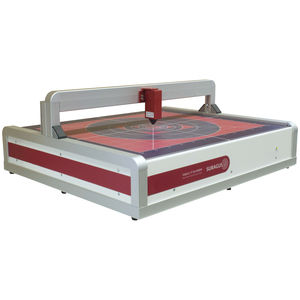
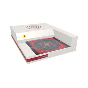
The EddyCus® TF map 2530 Series automatically measures the sheet resistance of large samples up to 300 x 300 mm² (12 x 12 inches) in non-contact mode. Upon manual sample positioning the device automatically measures and displays an accurate mapping of the sheet resistance across the entire sample area. The measurement settings allow easily and flexibly to choose between fast measurement times of below 1 minute or high spatial measurement resolution of more than 100,000 measurement points.
Highlights
Non-contact
Fast and precise measurement
High resolution mapping of conductive thin films
Imaging of substrates up to 300 x 300 mm (12 x 12 inches)
Characterization even of hidden and encapsulated conductive layers
Various software-integrated analysis functions (e.g. sheet resistance distribution, line scans, single point analysis)
Measurement data saving and export functions
Defect detection and coating analysis
Types
The device platform is available in different sensor configurations including eddy current sensors for electrical characterization or sensors for optical characterization. Variants of the measurement configurations involve the following options.
Characteristics
Technology: non-contact eddy current
Imaging by multipoint mapping
Positioning area: 300 mm x 300 mm
Sampling area: 300 x 300 mm
Recommended sample sizes: 1 inch to 12 inch or 25 to 300 mm
Software and Device Control
Very user-friendly software
Realtime mapping measurement
Easy-to-use statistical analysis options
Pre-defined measurement and product recipes (sizes, pitches, thresholds)
Line scan, histogram and area analysis
Black and colored image coding
VIDEO
Catalogs
No catalogs are available for this product.
See all of SURAGUS GMBH‘s catalogsRelated Searches
- Laser scanner
- Aeronautic laser scanner
- Non-contact laser scanner
- Aeronautic thickness gauge
- Thickness gauge
- Coating thickness gauge
- 3-axis laser scanner
- NDT thickness gauge
- Contact laser scanner
- Eddy current thickness gauge
- Digital display thickness gauge
- Glass thickness gauge
- Aeronautic crack detector
- Crack detector
*Prices are pre-tax. They exclude delivery charges and customs duties and do not include additional charges for installation or activation options. Prices are indicative only and may vary by country, with changes to the cost of raw materials and exchange rates.


