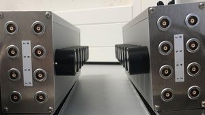
Glass thickness gauge EddyCus® TF lab 2020SRfilmnon-contactfor aeronautics

Add to favorites
Compare this product
Characteristics
- Applications
- glass, film
- Technology
- non-contact
- Other characteristics
- for aeronautics, for NDT
- Measuring range
2 mm
(0.08 in)
Description
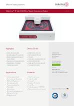
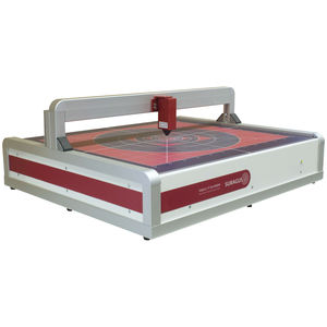
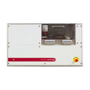
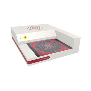
The EddyCus® TF lab 2020 Series allows manual single point measurements of conductive thin films and layer thickness measurement of thin metal layers in non-contact mode. The compact bench-top device is ideal for fast and accurate measurements of samples up to 200 x 200 mm² (8 x 8 inches). In addition to the measurement of thin conductive layers also doped wafers and conductive polymers can be analyzed.
Highlights
Non-contact real time measurement
Precise measurement of conductive thin films
Characterization of hidden and encapsulated conductive layers
Measurement data saving and export functions
Characteristics
Sheet resistance
Thickness measurement of metal layers
Single point measurement
Quality control, input and output control
Sample sizes: 10 x 10 mm² to 200 x 200 mm² (0.5 x 0.5 inches to 8 x 8 inches)
Measurement range: 0.1 mOhm/sq to 100 kOhm/sq
Applications
Coated architectural glass, e.g. LowE
Displays, touch screens and flat panel displays
OLED and LED applications
Smart glass
Graphene layers
Photovoltaic wafers and cells
Semiconductor wafers
Metallization layers and wafer metallization
De-icing and heating applications
Battery electrodes
Conductively coated paper and conductive textiles
VIDEO
Catalogs
EddyCus® TF lab 2020SR
2 Pages
Related Searches
- Laser scanner
- Aeronautic laser scanner
- Non-contact laser scanner
- Aeronautic thickness gauge
- Thickness gauge
- Coating thickness gauge
- 3-axis laser scanner
- NDT thickness gauge
- Contact laser scanner
- Eddy current thickness gauge
- Digital display thickness gauge
- Glass thickness gauge
- Aeronautic crack detector
- Crack detector
*Prices are pre-tax. They exclude delivery charges and customs duties and do not include additional charges for installation or activation options. Prices are indicative only and may vary by country, with changes to the cost of raw materials and exchange rates.


