Glass thickness gauge EddyCus® TF lab 4040SRfilmnon-contactfor aeronautics

Add to favorites
Compare this product
fo_shop_gate_exact_title
Characteristics
- Applications
- glass, film
- Technology
- non-contact
- Other characteristics
- for aeronautics, eddy current
- Measuring range
2 mm
(0.08 in)
Description
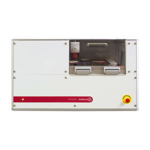
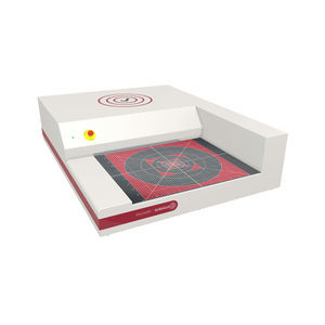
The EddyCus® TF lab 4040 Series is dedicated to non-contact single point measurements on medium sized substrates. The flexibly applicable bench-top device allows depending of its setup the precise manual measurement of sheet resistance, metal thickness, optical transparency or electrical (an)isotropy. Most common applications include the measurement of thin conductive transparent and non-transparent layers, wafers or metal sheets.
Highlights
Non-contact, real time, robust
Accurate and very repeatable measurements
High measurement quality without influence of:
Homogeneous contact quality
Passivation / Encapsulation
Roughness
No harm to sensitive layers
Precise measurement of
Conventional conductive thin-films
Grids and wire structures
Multi-layer systems
Hidden and encapsulated conductive layers
No wearing
Software guided manual mapping for systematic quality assurance
Many measurement data saving and export functions
Space saving smart monitor integration (for measurement per touch screen and data evaluation)
Software development kit test automation using customer programs
Types
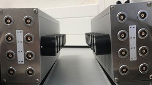
The device can be equipped with different sensors including eddy current sensors for electrical characterization or sensors for optical characterization. Variants of the device platform involve the following options.
VIDEO
Catalogs
EddyCus® TF lab 4040SR
2 Pages
Related Searches
- Laser scanner
- Aeronautic laser scanner
- Non-contact laser scanner
- Aeronautic thickness gauge
- Thickness gauge
- Coating thickness gauge
- 3-axis laser scanner
- NDT thickness gauge
- Contact laser scanner
- Eddy current thickness gauge
- Digital display thickness gauge
- Glass thickness gauge
- Aeronautic crack detector
- Crack detector
*Prices are pre-tax. They exclude delivery charges and customs duties and do not include additional charges for installation or activation options. Prices are indicative only and may vary by country, with changes to the cost of raw materials and exchange rates.


